

EOS Mitigation
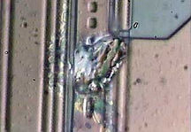
EOS Damage
"EOS is the number one source of damage to IC components" according to Intel*. Industry standards as SEMI E.176 and IPC-A-610 set acceptable voltage levels for sensitive components to no more than 0.3V peak. Such low damage levels comparing to 100V or 250V for ESD are due to the high energy that EOS-causing signals can inject into the device.
Perhaps the most damaging aspect of EOS is that often the damage is "latent," i.e. when the device or the board which is "wounded," not outright "killed" by excessive voltages and currents, passes the test, but then fails in actual use due to the weakened internal structure. Not only this adds to the cost and aggravates customer relations, it also threatens applications where a "failure is not an option."
A very significant source of EOS damage is EMI, or high frequency voltages and currents, in the manufacturing and handling processes. In the device and board handling and processing equipment EOS exposure due to EMI comes from the difference in voltage on grounded parts of equipment which are deemed "safe" by conventional practices and measurements.
* Intel® Manufacturing Enabling Guide, Section 3: ESD/EOS 2016
EOS Diagnostics and Mitigation
EOS is almost never gets to be specified, verified or addressed. If your best customer asks you: "what is EOS exposure to my components that I buy from you," would you be able to provide an answer? We can help you not just to provide this answer but more importantly, provide this answer to you before the customer asks the question.
For unpowered devices we will examine actual voltages and currents that your devices experience at every step of your process, analyze what may be causing it and provide recommendation on mitigation of EOS. Then we will verify that whatever was done actually works.
For powered devices, i.e. in test, we will work together with your test and tool engineers to find that elusive spike or glitch that causes latch-up and, ultimately, device damage
EOS Audit
Just like an ESD Audit, a comprehensive EOS audit focuses on actual EOS exposure to the devices in your process. All undesirable voltage and currents applied to the devices are analyzed and quantified and are compared with industry standards and recommendations - if you have your own requirements, we would consider them too.
Should EOS exposure be present in your equipment, we can work with your tool suppliers to mitigate such exposure so that you don't have to. We can work with your facility engineers to verify that power and ground you rely on are "clean" and safe for the devices.
EOS Program
You already have in place ESD program at your factory. You have requirements for every single component of ESD protection and your employees are properly trained. The problem is that it is not ESD, it is EOS that is "the number one source of damage to IC components" and you have nothing in place to provide adequate protection in your process for EOS exposure.
EOS program should be taken very seriously, addressing all aspects of EOS exposure of the devices at every step.
As someone who is intimately familiar with current developments on EOS at ESDA, working with relevant SEMI Standards in EMC contributing to IRDS, I can check compliance with these requirements and recommendations at your facility, as well as assist you in meeting and maintaining levels of EOS that won't affect your process and devices.
EOS Classes and Seminars
While ESD phenomenon is reasonably understood and addressed, EOS is not. A practical goal-oriented education on all aspects of EOS at different stages of manufacturing and handling would help your staff to deal with EOS in a planned and effective way backed by solid understanding of "why, what and how." BestESD principal, Vladimir Kraz, conducted classes with audience ranged from one-on-one to 350 attendees.
The classes can be conducted at your factory for the maximum coverage and effectiveness. Please contact us for details.